PForces and currents in carbon nanostructures
 Wednesday, 30 March 2011, 12:00-13.00
Prof. Pablo Pou
Dpto. de Fisica Teórica de la Materia Condensada, UAM
ABSTRACT:
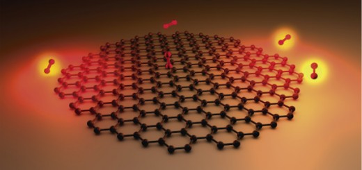
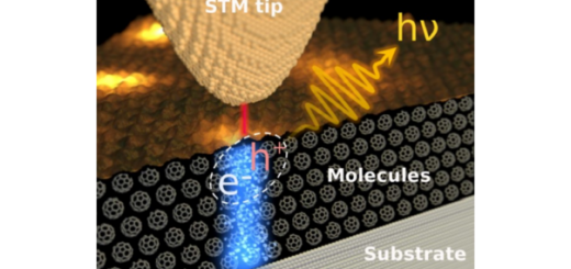
STM [1] and FM-AFM [2] have been used for many years to study low-dimensional carbon materials. The simple honeycomb structure shared by these materials represents both a perfect testing ground and a fundamental challenge for scanning microscopy imaging. Graphite can be imaged with atomic resolution with Scanning Probe Microscopy even in ambient conditions but, after 25 years of research, still there is no consensus whether the maxima in the atomic scale images correspond to atoms or to the hollow sites. We have carried out a study that combines DFT total-energy calculations with NEGF methods for electronic transport in order to determine the interaction and the tunneling current between a large set of SPM tips with nanotubes, graphite and graphene [3]. Our results explain the rich variety of image patterns observed in both AFM and STM experiments in terms of two factors: (i) the tip-sample distance and (ii) the chemical reactivity of the tip. Furthermore, we demonstrate, contradicting the usual interpretation, that short-range chemical forces and not van der Waals interactions are the responsible for the atomic-scale contrast on the FM-AFM images.
Finally, we have extended our study to defects in these materials, which, instead of a problem, result on novel and promising electronic properties. For example, vacancies in a graphene layer support localized magnetic moments [4]. We present a study of the forces and currents on a graphene layer on Pt considering explicitly the presence of vacancies [5].
[1] Park et al, APL 48,112 (1986)
[2] Holscher et al, PRB 62, 6967 (2000); Hembacher et al, PRL. 94 056101 (2005); Albers et al, Nat Nano 4, 307 (2009); Gross et al, Science 325, 1110 (2009)
[3] Ondraceck et al, PRL (2011).
[4] Ugeda et al, PRL 104, 096804 (2010).
[5] Ugeda et al, submitted to PRL (2011).


