Semiconductor nanostructures grown on GaAs nanoholes for quantum optical information technologies
 Wednesday, 7th March 2012. 12:00-13:00
Benito Alén
Instituto de microelectronica de Madrid, CSIC
ABSTRACT:
Single semiconductor quantum dots embedded monolithically in photonic or electronic devices are a fundamental resource for quantum information science and technology.[1] Individual charges and spins can be addressed in these systems through combined electrical and optical manipulation.[2] Quantum information processing tasks can be implemented using the individual spins of a quantum dot molecule as quantum bits.[3] Also, when embedded in a high quality photonic crystal microcavity, spins can be coherently mapped into single photons enabling quantum non-demolition optical read-out or long distance quantum communications.[4]
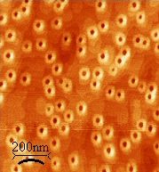
Despite the considerable progress done so far, standard fabrication methods are based on self-assembled processes which lead to the random nucleation of the nanostructures over the semiconductor substrate. This is a serious drawback for the deterministic and scalable fabrication of the building blocks mentioned above. In this talk, I will present how semiconductor nanostructures grown directly over pre-patterned substrates could in principle solve this problem. InGaAs quantum dots and quantum dot molecules grown directly on GaAs nanoholes will be presented and their optical and electronic properties will be discussed. [5-8]
1. Faraon, A. et al. Integrated quantum optical networks based on quantum dots and photonic crystals. New Journal of Physics 13, 055025 (2011).
2. Atature, M. et al. Quantum-Dot Spin-State Preparation with Near-Unity Fidelity. Science 312, 551–553 (2006).
3. Robledo, L. et al. Conditional Dynamics of Interacting Quantum Dots. Science 320, 772 –775 (2008).
4. Rakher, M. T. el al. Externally Mode-Matched Cavity Quantum Electrodynamics with Charge-Tunable Quantum Dots. Phys. Rev. Lett. 102, 097403 (2009).
5. Alonso-González, P. et al. Formation and Optical Characterization of Single InAs Quantum Dots Grown on GaAs Nanoholes. Appl. Phys. Lett. 91, 163104 (2007).
6. Alonso-González, P. et al. Formation of Lateral Low Density In(Ga)As Quantum Dot Pairs in GaAs Nanoholes. Crystal Growth & Design 9, 2525–2528 (2009).
7. Martín-Sánchez, J. et al. Single Photon Emission from Site-Controlled InAs Quantum Dots Grown on GaAs(001) Patterned Substrates. ACS Nano 3, 1513–1517 (2009).
8. Muñoz-Matutano, G. et al. Charge control in laterally coupled double quantum dots. Phys. Rev. B Rapid Comm. 84, 041308 (2011).