A Bright Nanolight for Plasmonic Circuitry
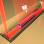
Figure: Schematic illustration of the proposed hybrid plasmonic platform for an on-chip nanolaser source. It consists of a GaAs nanowire positioned inside a 30 microns-long gold V-groove waveguide capable of coupling its lasing emission to the propagating plasmonic modes supported by the structure.
Article: published in Nano Letters by Javier Cuerda, Jorge Bravo-Abad and Francisco J. Garcia-Vidal, Department of Theoretical Condensed Matter Physics and IFIMAC researchers.
The need of ever faster and powerful data processing and communication technologies, as well as for ultrasensitive and compact sensors is playing a crucial role in the advance of novel on-chip optical devices. It is a matter of time before integrated photonic circuits will become inherent in our daily lives in a similar way that electronic circuits did with the development of the transistor. Currently, one of the main goals in nano-photonics research is being able to integrate all the key necessary building blocks on a same chip, including the light source, transmission lines, modulators and detectors. Small on-chip lasers have emerged over the last decade as an ideal solution for the light source integration, however the main challenge is to efficiently couple their emission into the small footprint components.
Now, in a recent Nanoletters publication, a group of researchers from the Departamento de Física Teórica de la Materia Condensada and the Condensed Matter Physics Center (IFIMAC) at the Universidad Autónoma de Madrid, together with researchers from the Institute of Photonic Sciences (ICFO), the Laboratory for Semiconductor Materials at the EPFL in Switzerland, the Technical University of Denmark and the Center for Nano Optics in Denmark, report on the realization of a novel ultracompact hybrid nanolaser source operating at room temperature consisting of semiconductor nanowire (NW) lasers directly integrated with wafer-scale lithographically designed plasmonic waveguides.
To achieve this, the researchers used epitaxially grown GaAs NWs with diameters at least ten times smaller than a human hair and a few microns in length, which provided both the gain medium and the cavity geometry required for the lasing emission. The NWs were then transferred from their host substrate onto a silicon chip containing gold V-groove (VG) plasmonic waveguides, which support a special type of surface plasmons with sub-wavelength lateral electromagnetic field confinements and good propagation characteristics, namely the channel plasmon polaritons (CPPs). Later, by means of micro and nanomanipulation techniques, the researchers deterministically positioned individual NWs at the bottom of the VG channels, forming the so-called NW-VG hybrid nanolaser.
Lasing action and emission coupling to the plasmon CPP waveguide mode was observed upon pulsed illumination of the NW. Furthermore, rigorous theoretical simulations revealed that the lasing action in these devices was enabled by a hybrid photonic-plasmonic mode supported by the NW-VG geometry. The demonstrated system exhibited an unprecedented transfer efficiency of the lasing emission into the CPP waveguide mode of nearly 10%. This benchmark result was possible thanks to the good overlap between the hybrid plasmon lasing mode and the subwavelength confined CPP mode of the waveguide.
The authors envision that the unique features of the developed integrated source will provide the means to build high-sensitivity chemical or bio-sensing platforms powered by an integrated nanolaser. Future directions will also focus on the development of electrical injection as well as the integration of other on-chip components along the VG to build functional photonic circuitry, for example, in quantum optics experiments employing single quantum emitters coupled to the CPPs or integrating electro-optic elements in high-speed plasmonic modulators for data communications, which overall can bring us one step closer to future hybrid photonic-plasmonic circuit platforms. [Full article]


